Address
304 North Cardinal St.
Dorchester Center, MA 02124
Work Hours
Monday to Friday: 7AM - 7PM
Weekend: 10AM - 5PM
Address
304 North Cardinal St.
Dorchester Center, MA 02124
Work Hours
Monday to Friday: 7AM - 7PM
Weekend: 10AM - 5PM
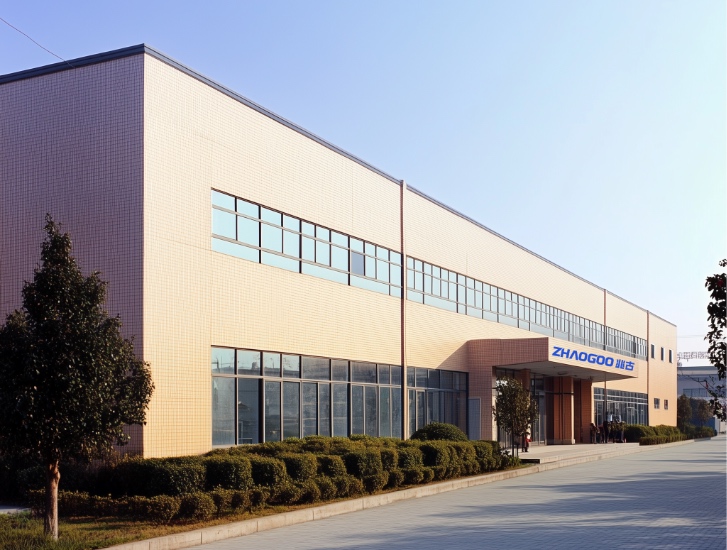
Founded in 2012 and headquartered in Shenzhen, China – the global epicenter of electronics innovation – ZHAOGOO has rapidly evolved into a trailblazer in advanced printed circuit board (PCB) solutions. With a workforce of 120 highly skilled professionals operating across a sprawling 3,872 m² state-of-the-art facility, we specialize in high-density flexible PCBs and mission-critical rigid-flex hybrid boards that power next-generation technologies. Our strategic Hong Kong office bridges international operations, ensuring seamless cross-border collaboration with partners worldwide.
Key Metrics
ZHAOGOO engineers flexible circuits capable of 500,000+ dynamic flex cycles (IPC-6013D compliant) and rigid-flex boards with 20-layer hybrid constructions, enabling:
Our Digital Thread Production System integrates:
| Equipment | Capability Breakthrough | Industry Benchmark |
|---|---|---|
| CNC Laser Drilling | 25μm positional accuracy for HDI layouts | ±5μm超越JIS C 5016标准 |
| Yamaha YSi-V Autoline | 160,000 CPH placement with 15μm fiducial alignment | 支持01005元件(医疗植入级精度) |
| 3D X-Ray Inspection (Dage XD7600) | 5μm void detection in BGA joints | 满足NASA-STD-8739.4航天焊接规范 |
| AOI with AI Defect Learning | 99.97% fault recognition rate across 22 IPC defect categories | 学习周期缩短至15分钟/新型号 |
Every substrate undergoes blockchain-tracked quality provenance verification:
| Client | Project Signature | ZHAOGOO Value Proposition |
|---|---|---|
| Huawei | 5G Massive MIMO Antenna Flex-Rigid Stacks | 38% weight reduction vs. traditional FR4 |
| DJI | Foldable Drone Motor Control Flex Circuits | 270° twisting endurance (IPC-2223C 10X) |
| Samsung | Foldable Display FPC with 0.3mm bend radius | 20kV ESD protection (IEC 61000-4-2 L4) |
2025 Quantum Leap Initiative
ZHAOGOO engineers actively contribute to IPC-6013E Flexible Circuits Standard revisions and sponsor the IEEE Heterogeneous Integration Roadmap. Our Shenzhen facility houses an Open Innovation Lab for startups developing IoT and wearable technologies.
Contact
Shenzhen HQ: 310 Tongfang Center, Xinqiao Street, Baoan,Shenzhen
Hong Kong Office: 4/F Central Ind Bldg 89-91 Ta Chuen Ping St Kwai Chung
Web: http://www.zhaogoo.com
Email: [email protected]
I WANT TO INQUIRE


PCB-Centric Expertise: Delivering Tailored Products & Services for Your Needs
Empowering Innovation: Rapid PCB Prototyping with Flexible Assembly Support for R&D Teams.
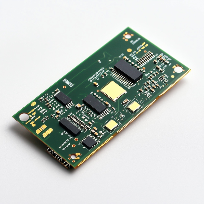
Includes: Flexible PCBs, Rigid-Flex PCBs, FR4 PCBs, Aluminum/Copper-based PCBs, Rogers/Teflon(PTFE) High-Frequency PCBs
13 fully operational lines for SMT and DIP processes, equipped with 8 Yamaha high-speed SMT placement systems.
Submit existing schematics or provide functional specifications, and our team will deliver compliant circuit designs.
Dedicated Warehouse with 12,510 Standard Components & Global Market Integration for Agile Procurement.
Post PCB assembly, we offer integrated enclosure assembly and full product validation services.
Quality Control
From raw material inspection to final testing, stringent quality control standards ensure 0 PPM (Parts Per Million) defects.
Multi-Industry Certified: ISO 9001 • IATF 16949 • AS9100 • ISO 13485 • NADCAP
Compliant with IPC-A-600, IPC-6012, and IPC-6013 standards, and certified to UL 94 and UL 796.
REACH SVHCs <0.1% | RoHS 3 Compliant | ISO 14001:2015 Certified.
Our PCB solutions are engineered for versatile applications, empowering your products with thinner profiles, lighter weight, comprehensive functionality, and enhanced reliability.
NEV Optimized FPCBs
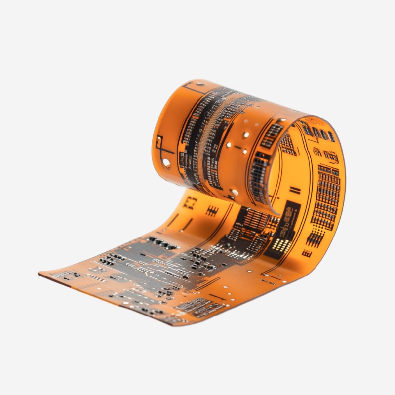
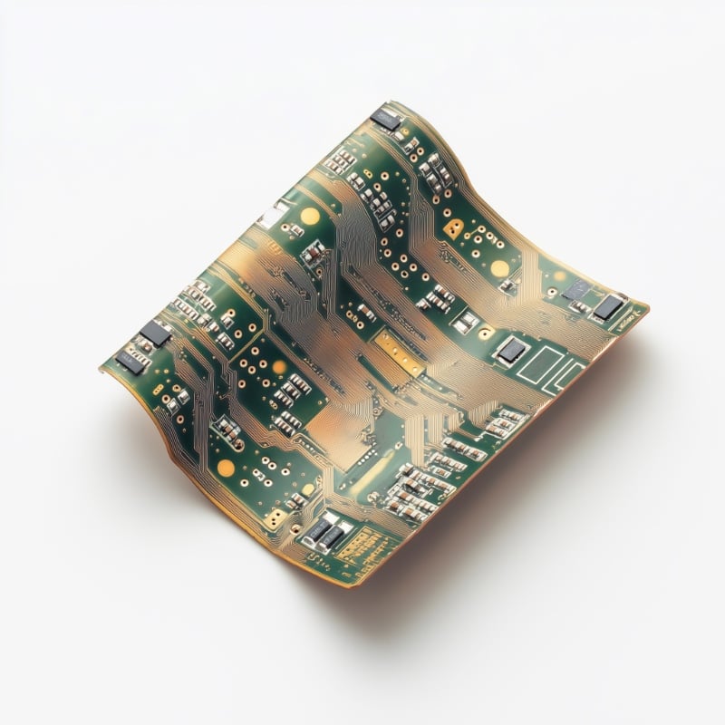
FPC (Flexible PCBs)
PTFE (Teflon®) High-Frequency PCB
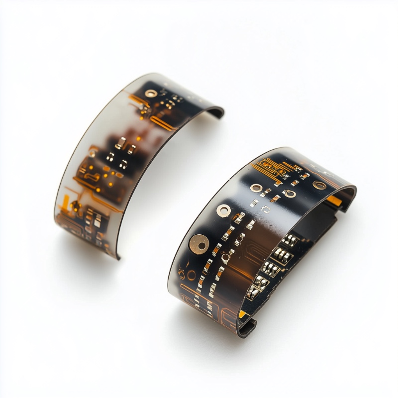
Wearable-Optimized FPCBs
we manufacture high-quality Flexible PCBs and Rigid-flex PCBs that meet the most stringent requirements of IPC-6012/3 standards.

Production Capacity
Active Customers
Number of employees
Factory Floor Area
Each year prior to the holiday season, we conduct an annual client review to continuously enhance our service quality and responsiveness.
Abigail
Electronics Designer
“All I needed was FPC. From the time I sent the PCB information to ZHAOGOO’s email, including the quotation and receiving the DHL waybill number, it only took 3 days in total, and this product completely met my expectations.”
John Wilson
Business Owner
“After 8 years of cooperation with ZHAOGOO, we have become friends. I go to China every year and have seen ZHAOGOO continue to grow stronger. Now we purchase all the rigid-flex PCBs we need from their company.”
Michael
Purchasing Manager
“I am from Utah, USA. We only provide PCB drawings, and everything else is completed by ZHAOGOO, including the purchase of electronic materials and SMT. So far, there has been no quality risk.”